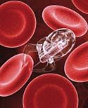
Finland and China team up in nanotechnology
NanoChina
Finland's national nanotech initiative (FinNano) is rapidly advancing on the international scene. After kickstarting cooperation with Russia last week, FinNano is now sowing seeds in China.
Finland is a leading partner in the Europan Union's nanotech group NMT, and directs the EU's material technology group MATERA.
The partners in Finland–China NAMI cooperation aim to create world class research and put Sino–F innish nanotech products on the market together by 2010.
The Chinese Minister of Science and Technology (MOST) Dr. Wan Gang and Vice Minister Dr. Shang Yong joined in the celebration of the opening of China International Nanotech Innovation Cluster (CINIC) in Suzhou on Saturday. Finland has set foot in Suzhou, signing agreements for nanotechnology development and commercialisation.
Mr. Juho Rissanen, the Beijing representative of Tekes and counsellor of science and technology at the Embassy of Finland, gave an opening speech in Chinese informing the new MOST Minister on the current status of Finland-China nanotech cooperation. Dr. Markku Lämsä, who leads Finland's nanotech programme, signed a cooperation agreement with Suzhou nanotech cluster. Represented by Mr. Jaani Heinonen of Tekes Shanghai office and the Consulate General of Finland, the Finnish Technical Research Centre VTT also signed a cooperation agreement with Suzhou.
"The willingness to team up and the amount of joint projects proposed clearly show the demand for deeper collaboration between China and Finland in the area of nanotechnology. The Sino–Finnish NAMI Nanotech Program can also positively increase the exchange of know-how between the European Union and China", says Dr. Lämsä.
The China–Finland NAMI (Nanotechnology Strategic Mutual Cooperation Initiative) was signed in Beijing in January 2007, and more than 30 project proposals and expressions of interest have been collected so far. The first cooperation projects under the NAMI programme have been launched in October.
Finland is the first country to sign a national level strategic cooperation agreement with China on nanotechnology. The new Finnish technology programme on functional materials, with a budget of 200 million euros, was introduced to the Chinese Ministry of Science and Technology last Monday in Beijing. It is expected that still more cooperation projects will be generated under this new programme, to be implemented under the NAMI framework. Both the national nanotech programme and functional materials programme are funded and directed by Tekes, and coordinated by Spinverse Inc., a private Finnish technology consultancy.
Ambitious objectives for cooperation
Finland–China NAMI cooperation aims at increasing the competitiveness of industrial sectors in the two countries. The industries include information and communication technologies, pulp and paper, chemicals, metals and other materials, diagnostics and healthcare. The production of energy using new technologies such as solar cell and fuel cells may also be considered.
In Finland, nanotechnology is one of the focus areas of national innovation policy, with extensive public and private investments. The Finnish Nanoscience and Nanotechnology Programme FinNano is a coordinated action on a national level to increase the expertise in science and technology. Finnish public funding organisations are investing more than 120 million euros in nanoscience and nanotechnology programmes between 2005 and 2010.
Launch of Joint BMBF "Nanoanalysis" Project for Chip Development
From Nanoforum
DRESDEN, OBERKOCHEN/Germany, 06.11.2007.
The companies AMD, Carl Zeiss SMT and Qimonda are launching a cooperation within the framework of the joint “Nanoanalysis“ project which is funded by the German Federal Ministry of Education and Research (BMBF) with a sum of 12 million euros. The partners are working together on new analytical and characterization methods required for the development of the next chip generation. This strengthens the competency of the Dresden microelectronics site, particularly in the fields of semiconductor analysis and metrology.
As announced today by Dr. Wolf-Dieter Lukas, Head of the BMBF Department “Key Technologies – Research for Innovations“, the strategic setup and expansion of microelectronics competency centers is an important goal of the BMBF IKT2020 program. “Only by setting targeted priorities in research funding will we succeed in maintaining Dresden’s leading role in high-tech chip production and in further expanding it through such innovative approaches as here in the field of nanoanalysis.“
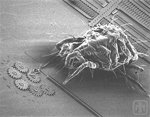
The newly founded “Carl Zeiss Innovation Center Dresden“ is an important module within the joint “Nanoanalysis“ project. Here, ultrahigh resolution particle beam systems are being installed which use electron and ion beams instead of light. These systems enable the imaging, analysis and processing of specimens down to the level of individual atoms. In this way, they are playing a decisive role in the characterization of three-dimensional semiconductor structures and in the development of new materials for chip fabrication. “With its Innovation Center, Carl Zeiss SMT is becoming involved in ‘Silicon Saxony’, Europe’s leading microelectronics cluster. Not only is the cluster being strengthened in its function as a research location, but the ongoing development of the local semiconductor industry is also being promoted”, explains Dr. Dirk Stenkamp, Member of the Carl Zeiss SMT Board of Management.
“As a manufacturer of innovative microprocessors, we are faced with the challenge of producing increasingly complex structures with smaller and smaller dimensions and with maximum yield“, says Dr. Udo Nothelfer, Vice President AMD Fab 36. “Therefore, process control at an atomic level plays a key role. Through our joint work in the Carl Zeiss Innovation Center Dresden, we have access to leading edge electron and ion microscopes and believe we can therefore further accelerate the introduction of new technologies. The experience gained in industrial utilization may be incorporated at an early stage in the development of future analytical systems.“
“With the structure dimensions now achieved, current storage cells can only be seen under the electron microscope“, says Frank Prein,
Managing Director Qimonda Dresden and Senior Vice President Technology Qimonda. “Only through the consistent enhancement of the analytical and measuring methods will it be possible to master the future challenges posed by the development and production of state-of-the-art storage technologies. Through the diversified integration of research partners, Qimonda will use the excellence of the research location for its technology competency center in Dresden within the framework of the joint ‘Nanoanalysis’ project and expand and strengthen its scientific network.“
In addition to the cooperation partners AMD and Qimonda, the “Carl Zeiss Innovation Center Dresden“ is available to all interested firms and institutes in the Dresden area. In particular, all partners of “Silicon Saxony”, e.g. the Dresden Technical University or the Fraunhofer Center Nanoelectronic Technologies CNT, can resolve application problems in the field of nanotechnology.
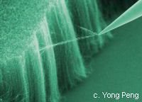
Faster and more efficient thanks to "defects"
From Nanoforum
Smaller, faster, more efficient: BASF research scientists are helping to revolutionize the future world of telecommunications - with the aid of three-dimensional photonic crystals. In a three-year project, BASF is researching into the development of these crystals together with partners such as Hanover Laser Center, Thales Aerospace Division, Photon Design Ltd., the Technical University of Denmark and the Ecole Nationale Supérieure des Télécommunications de Bretagne. joint ‘Nanoanalysis’ project and expand and strengthen its scientific network.“
Monday, 17 December 2007
Nanotech Week European News
Subscribe to:
Post Comments (Atom)


No comments:
Post a Comment