Feb 15, 2008
By Belle Dumé
A new bottom-up assembly method to make large-area nanoelectromechanical (NEM) arrays - each containing over 2000 single-nanowire resonators has been developed by researchers in the US. The technique is a practical alternative to top-down fabrication and the arrays could be used as multi-analyte biosensor chips.
NEM resonators are good candidates for making chip-based sensor arrays because they can sense ultralight masses. However, it is difficult to integrate nanowires into large arrays using traditional top-down techniques, such as optical lithography.
The new bottom-up technique was devised by Theresa Mayer of Pennsylvania State University and colleagues, and involves assembling thousands of chemically functionalized nanowire resonators and integrating them on a silicon chip. The finished nanodevices can bind specific biomolecules and so serve as sensors.
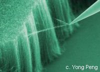
Mayer and colleagues begin by applying an alternating voltage between pairs of metal guiding electrodes patterned on a silicon chip. This produces spatially confined electric fields that attract the nanowires placed on the chip to specific regions.
The nanowires then align and drop one-by-one into wells patterned onto a sacrificial dielectric layer coated on top of the electrodes. The wells are slightly larger than the nanowires and are placed a few microns apart. This determines nanowire density, which can be as large as 1 million devices per square centimetre.
Next, the researchers deposit metal contacts onto the chip until the contacts fill small gaps in the sacrificial dielectric layer at the ends of each well. This mechanically and electrically connects the nanowires in the wells to the chip surface. Eventually, this technique will be used to connect to underlying silicon circuits, says Mayer.
Finally, the sacrificial layer is dissolved and any misaligned nanowires, not securely fastened to the chip by metal contacts, are washed away. This leads to a higher yield of assembled single nanowire devices over large chip areas.
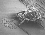
"We used this assembly method to fabricate arrays of cantilevered silicon and metal nanowire resonators," Mayer told nanotechweb.org. "However, it is versatile and can be used to fabricate other types of nanowire-based devices as well."
The technique may also allow integration of many different types of nanowires functionalized to detect different target biomolecules made in large batches on fully processed silicon logic chips, added Mayer.
The team is now trying to extend its assembly technique to allow selective positioning of various types of nanowires in different locations on the chip. This will allow multiple biomolecule targets to be detected on the same chip. "We are also investigating new approaches to make an all-electrical interface to the silicon chip," said Mayer.
The work was reported in Nature Nanotechnology.
About the author
Belle Dumé is contributing editor at nanotechweb.org


No comments:
Post a Comment