Thursday, 28 February 2008

Nanotech Week: European News

A code of conduct for responsible nanosciences and nanotechnologies research

European Commission on Nanotechnology

7th February 2008

The COMMISSION OF THE EUROPEAN COMMUNITIES has drawn up a code of conduct for responsible nanosciences and nanotechnologies research. It was recognised “the need to foster synergies and cooperation between all nanosciences and nanotechnologies stakeholders, including the Member States, the Commission, academia, research centres, industry, financial bodies, non-governmental organisations and society at large.”

This ten page report is the result of concerns which have been raised over both nanotechnology and nanoscience. These concerns were made clear during a two day conference held at the Royal College of Surgeons (Please read Investing in Medical Nanotechnologies II - Review 7 December 2007) in November. There was confusion over varying definitions as to what are nanotechnology and nanoscience as well as “the risks of nanoparticles, products and technology”. One audience member had three different codes of conduct on his desk. All were unanimous in the need for a code of conduct.


From Qinetiq to Intrinsiq Via Brownian Dithering


Cientifica

25 Feb 2008

Finally, someone decided what to do with UK nanotech stalwart Qinetiq Nanomaterials. The new big idea is to change its name to Intrinsiq Materials and rebrand it as a company operating in the hitherto unheard of “Clean Tech and Wellness sector.”

After years operating on the edge of UK defence giant Qintetiq, the parent company has finally decided to pop in another five million pounds through Cody Gate Venture and appoint a new CEO who bears a startling resemblance to the one that they let go 18 months ago, something that seems to have been omitted from the rebuffed CV.

While all the rebranding of nanotech as Cleantech is fun to watch, is this the first company to actually change its name to remove the word ‘nano’?


Oxonica Goes Biotech

Cientifica

24 Feb 2008

While on the subject of rebranding former nanotech companies, Oxonica is now a biotech company according to the Oxford Mail. This is Money had a rather less flattering description of the company as a “Bombed-out industrial materials group” which announced that its fuel catalyst does work after all and that UK bus operator Stagecoach, who own some 4% of the company, would buy 750,000 pounds worth of the stuff.

While there is no doubt that fuel catalysts do have some effect, the variability of the results so far indicates that factors such as driving style, fuel and engine type also have some effect. The Stagecoach news doubled the market cap of the company, with their 750k adding something like 14 million pounds to the company’s worth, which shows how volatile things are down at the bottom end of the market.

Nanotech in the Desert, Six Years On


Tim Harper, Cientifica Ltd


Earlier in the month I popped over to Palm Springs to visit IBFs Nanotech Investing Forum.

Six years ago I gave a keynote speech at the first IBF Nanotechnology Investing Forum in which I gave my vision for the future of nanotechnology. My message was simple, “there is not, and there never will be a nanotechnology industry.” This was very bad news for all of the people who had staked their career and/or a few million dollars on profiting from the next industrial revolution and there was quite a debate about whether that view was rational or cynical.

At this years 7th annual NIF, which had shifted a few miles east to Indian Wells to see what had changed. Over dinner the night before the conference I was told by a couple of people not to say anything bad about the state of the nanotech industry “it’s hanging by a thread right now” was one remark that was repeated a few times, and a number of people remarked that if the Nanodynmics IPO failed then it was all over.

Well it did, and it isn’t. What I did notice was that while most VCs are stampeding in the direction of clean tech, there were plenty of good looking companies applying nanotech to a wide range of industries, and making money too. Fortunately, with the less choosy VCs out of the way there is no need for ridiculous valuations or draconian term sheets these days, making the event far more pleasant than many of the early ones where people were climbing over each other to ‘own’ the nanotech revolution.

Someone once described venture capitalists to me as carnivorous sheep. When an opportunity arises they all make a lunge for it at the same time and rip it, and each other to shreds in the feeding frenzy, then its on to the next one.

Monday, 25 February 2008

Events: Biopharmaceutical Nanotechnology

Biopharmaceutical Nanotechnology
Targeting Nanotech Developments in Drug Delivery, Discovery and Therapeutics to Enhance Your Commercial Business Strategies

March 31 - April 1, 2008 · The Café Royal, London, UK

With the EU Seventh Framework Programme contributing approximately €600 million per year to bionanotechnology developments until 2013 - can you really afford not to claim your stake in this multi million pound industry?

What will I gain?

There have been many opportunities globally to discuss the theory, but where are the practical, commercially applicable lessons learned by your peers? Whether you are new to nanotechnology or an industry expert, this event will empower you to:

  • Stay competitive by applying the experience of key industry players who have used nanotechnology in the administration of drugs
  • Discover how nanotechnology combines drugs and devices to increase your product efficiency
  • Gain expert knowledge on the best ways to implement drug discovery techniques into your business processes
  • Incorporate latest therapeutic developments into your product pipeline
  • Enhance your commercial business strategies by employing the latest techniques discussed by the industry experts
Click here for a complete list of Biopharmaceutical Nanotechnology 2008 speakers

Register

Nanotech Week: European News

Colybris orders MEMS production systems from EV Group

Small Times

February 25, 2008

EV Group, which supplies MEMS and nanotech manufacturing equipment has received a multiple system order from Colibrys, a Swiss MEMS sensor supplier.

This follow-on order is for one EVG520 semiautomated wafer bonding system and two EVG620 fully automated mask/bond aligners.

One bonder and aligner tool set was installed at the Colibrys manufacturing facility in Stafford, Texas in January, while the other will be installed at the company's headquarters in Neuchatel, Switzerland before the end of the first quarter of 2008.

Follow-on orders like this helped EVG realize a 30 percent overall increase in both revenue and order intake in 2007, the company announced in a news release.


Steinmeyer's new manipulator stage targets nano, micro

Small Times

February 25, 2008

Steinmeyer Inc. has released its new high precision micro manipulator stage, MT 130-50-DC, geared toward nanotechnology, metrology, biomedical, and robotics applications.

Manufactured from high strength anodized aluminum, the standard table offers travel of 50 mm with positioning accuracy of 10 µm (micrometer), straightness/flatness runout of +/- 1µm and repeatability of +/- 1µm. With a sleek low profile design, it has a square footprint of 130 mm x 130 mm, height of 43 mm and weighs only 1.8 kg, the company announced in a news release.

Features include reloaded cross roller bearings, precision ground ball screw, limit switches, and integrated dc motor with rotary encoder. This product can be provided as a XY stage and can also be configured as a XYZ system-model MP 130-50-DC as a further enhancement. Motors, encoders and cabling are all hidden inside the table's body.

Motor, limit switch and encoder interface are via SUB-D connectors located in a single area. This stage is suited for semiconductor metrology, biomedical, miniature robotics, and laser industry applications, the company says.

Thursday, 21 February 2008

Casting a long line, A new way of making seriously long, seriously thin fibres

The Economist (print edition)

Feb 14th 2008

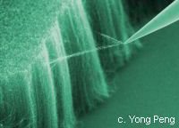
TINY fibres, a ten-thousandth of the diameter of a human hair, can be used to produce materials with novel electrical, optical and mechanical properties—at least in theory. But before engineers are able to turn them into practical applications, such nanofibres (which have a width of a few nanometres, or billionths of a metre) need to be fabricated into wires, strips, tubes and other components. That, in turn, means making them reliably and in large quantities. And a new production method developed by Min-Feng Yu and his colleagues at the University of Illinois may make this possible.

At the moment nanofibres are made in a variety of ways, none of which is entirely satisfactory. One uses condensation and evaporation, and is rather like some of the steps employed to make the fine structures on silicon chips. Screen-printing techniques are also being developed for some materials. A third trick relies on a system known as electrospinning, which dates back to the 1930s. In this, an electrically charged syringe squirts a polymer mixed with a solvent towards an oppositely charged electrode. The voltage difference causes a jet of the solution to stream from syringe to electrode. On the way, the solvent evaporates and the fibre solidifies. The technique works well enough, but the fibre that piles up on the receiving electrode tends to break up on arrival. It can end up looking like a plate of spaghetti.

By comparison, the fibres made by Dr Yu are nice and straight—and also astonishingly long. Most nanofibres are only nanometres in length as well as width, but the longest one made by Dr Yu stretches for half a metre—and he only stopped there because he got fed up with winding it up on a spool only a few millimetres in diameter. In theory, his method should be able to produce nanofibres of any length.

That method relies, like electrospinning, on dissolving the stuff that is to become the fibre in a solvent. The tip of a micropipette 100 nanometres in diameter is used to draw up the beginning of the thread and pull it across a surface on which it can dry. As the solvent evaporates, what is left behind solidifies. After that, it is simply a question of reeling in the prey. As long as the thread does not break, it can be drawn. And by moving the pipette both horizontally and vertically it is possible to make three-dimensional patterns with more structure than a bowl of spaghetti. That means component-manufacture should be possible.

According to Dr Yu, his method will produce fibres at the rate of 3mm a second, which bodes well for turning it into an industrial process. It should thus provide an economical way of making nanofibres from a variety of materials, provided only that those materials are soluble in something that evaporates reasonably fast.

It should also allow some novel nanofibres to be produced for researchers to experiment with. One possibility Dr Yu foresees is to incorporate fibres into materials such as blocks of plastic, and then dissolve them away to create tiny channels through which fluids could flow. That would make so-called labs-on-a-chip, which are used for some sorts of chemical analysis, easier to fabricate. Another idea would be to make those embedded fibres from pairs of materials which, when laid together within a substance, may be made to react together to produce a composite with useful electrical or mechanical properties. And, if all else fails, at least it makes an entertaining alternative to fishing.

Monday, 18 February 2008

Nanotech Week European Finance News

Small Times


D-Wave secures $17M Series C for quantum computing

February 4, 2008

D-Wave Systems, developer of quantum computers targeted at commercial applications, has announced the closing of a $17 million Series C financing. The round was led by International Investment and Underwriting (IIU) of Dublin, Ireland and was strongly supported by existing investors. D-Wave will use the funds for product development, operations and business development activity.

Our vision is to make quantum computing power available globally and to accomplish this requires a network of international partners," said D-Wave CEO Herb Martin.

D-Wave is the first company to announce the development of a commercial quantum computer and has twice publicly demonstrated prototype systems running real-world applications, the company said.

The D-Wave machine is intended to be deployed as a co-processor, which will provide acceleration to applications executing on classical digital computer systems.

D-Wave's system will be available for on-line access in early 2009 and will be useful for accelerating high value applications involving discrete optimization, pattern matching, machine learning and constrained search with preferences. Such applications are found throughout the operations research, life sciences, finance, travel, chemical and petrochemical industries. Applications in quantum simulation and electronic design automation will follow soon thereafter, the company said.

The latest financing round was fully subscribed by existing investors Draper Fisher Jurvetson (DFJ), GrowthWorks Capital Ltd, BDC Venture Capital, Harris & Harris, bcIMC and Pender Fund.


PSivida's pSiNutria business sold to Intrinsiq

January 25, 2008

pSivida Ltd. (Nasdaq: PSDV), a nanotech-based drug delivery company, has sold the assets of its wholy owned subsidiary, pSiNutria Ltd., to Intrinsiq Materials, a U.K.-based venture capital backed company.

pSiNutria was established in December 2005 to develop applications of the company's BioSilicon technology for the food industry.
As part of the deal, Intrinsiq will make a series of payments totalling $1.23 million in the first year following this closing of the transaction, then about $3.9 million over the next six years.

Protagen raises $1.5M to expand protein biochip unit

January 23, 2008

Protagen AG has announces the closing of an interim financing round of €1 million (about $1.5 million) to expand the company's protein biochips business unit.

The capital raised in this round has come from existing institutional investors, MIG AG and Co KG Beteiligungsfonds 3, Munich, and S-Venture Capital Dortmund GmbH, as well as from a new investor, Kreditanstalt für Wiederaufbau (KfW). This latest funding brings the total amount of venture capital financing raised by Protagen since 2004 to €5.3 million (about $7.8 million).

The UNIchip protein biochip range was launched onto the market in September 2005, and has experienced increasing demand from biotech and pharmaceutical companies, the company said in a news release.

MEMSCAP's Q407 earnings report reveals sustained profitability

January 21, 2008

France-based MEMS technology provider MEMSCAP has announced its earnings for the fourth quarter ending December 31, 2007. Among the main achievements reported are:

  • Highest quarterly revenue in U.S. dollars of the whole group history;
  • Profitability over nine consecutive months;
  • Second quarter in a row of operational profitability;
  • IntuiSkin annual revenue multiplied by four year to year.


Events: 3rd International Conference on Nanotechnology and Smart Textiles for Industry, Healthcare and Fashion

19 March 2008, Royal Society, London

Find out about the latest innovations being used to bring imaginative, exciting and novel properties to textiles for fashion and industry. These range from scent-embedded textiles, stay-clean textiles, textiles with displays and textiles that can change colour, to lightweight textiles that are so strong they can withstand the impact of a bullet.

For more information visit www.nano.org.uk/events or contact gemma.mcculloch@nano.org.uk

Nanotech Week: European Commision News

Nanoforum

Call for Scientific Data on Applications of Nanotechnology and Nanomaterials used in Food and Feed

The European Commission has requested an initial scientific opinion from EFSA relating to the risks arising from nanoscience and nanotechnologies on food and feed safety and the environment. The request also asks to identify the nature of the possible hazards associated with actual and foreseen applications in the food and feed area and to provide general guidance on data needed for the risk assessment of such technologies and applications.

European Commission adopts Code of Conduct for Responsible Nanosciences and Nanotechnologies Research

Europe is in the vanguard of the emerging field of nanosciences and nanotechnologies (N&N), a developing field of science with the potential for major positive impact economically, socially and environmentally. Nevertheless, knowledge gaps remain about the impact of these technologies on human health and the environment, as well as issues relating to ethics and the respect of fundamental rights. This is why the Commission is today recommending to the Member States to adopt a Code of Conduct to govern research in this field.

European Commission gives grant to investigate transatlantic oversight of nanotechnology

Researchers at the London School of Economics and Political Science (LSE), Chatham House, Environmental Law Institute (ELI) and the Project on Emerging Nanotechnologies (PEN), an initiative of Woodrow Wilson International Center for Scholars and The Pew Charitable Trusts, have been awarded a $587,000 European Commission grant to conduct an international research project on regulating nanotechnologies in the European Union and United States.

Events: Nanomechanics for NEMS: scientific & technological issues


26-27 June 2008, Minatec, Grenoble, France

A workshop of the Observatory for Micro & NanoTechnologies
This workshop is devoted to a worldwide state-of-the-art on NEMS and nanomechanics. During two days, the most recognised leading researchers will display the current state of research on fundamental topics and associated technological developments, challenges to overcome, main teams involved, applications & market to be aimed. Through four lively sessions, leaving enough time to questions and debate, chairmen and speakers will outline a complete and synthetic view of the subject. This workshop was elaborated with the help and participation of Prof. M. Roukes (Caltech).

For more information visit: www.omnt.fr


Events: Nanotech Northern Europe 2008

23-25 September 2008, Bella Centre, Copenhagen, Denmark

Nanotech Northern Europe 2008 has opened its call for contributions. To be considered, for an oral or poster presentation, please submit an abstract via the event website at www.nanotech.net. The deadline for submissions is 29th February 2008. Topics include:

  • Sustainable solutions for energy and environment
  • Nanotechnology-enabled ICT
  • Nanobiotechnology and nanomedicine
  • Nanotechnology and Food
  • Safety and Risk Management

For more information please visit www.nanotech.net

Nanotech Week: European News

Nano.org

TU Delft invests 10 million euro in bionanoscience

The TU Delft launches a new Bionanoscience Department, which will be part of the Kavli Institute for Nanoscience.

The new department will work together with the existing departments of Nanoscience and Biotechnology, and will count 15 top scientists in the coming years. A strategic collaboration with the European Molecular Biology Lab EMBL will also be developed.

Nano-Tera.CH gets a boost

The EPF Council has decided to allocate 40 million francs to the Nano-Tera.CH initiative (5 million in 2008, 8 million in 2009 and 13.5 million in 2010 and 2011).
The nano-tera program is centered on the application of micro/nano-technologies to embedded systems design, with the goal of improving human conditions through the monitoring of the human body and the environment. The total funding for this program, on the order of 60 MCHF, will support multidisciplinary projects to create complex systems for health, security and environment.
This decision is excellent news, not only for researchers in this domain, but also for industrial partners, and it will be an opportunity to showcase Swiss dynamism in this area. The program, coordinated by EPFL professor Giovanni de Micheli, will be officially launched January 28 in Bern.

The MONA Nanophotonics Technology Roadmap now available

During 2 years (2005-2007), the MONA ("Merging Optics and Nanotechnologies") consortium has been working through workshops, symposia and expert interviews at establishing a roadmap for photonics and nanotechnologies in Europe.

Nanosafe2 releases its first dissemination report

This first report is about conventional protective devices such as fibrous filter media, respirator cartridges, protective clothing and gloves and their efficiency against nanoaerosols.

Nano2Life - The European Landmark in Nanobiotechnology

Nano2Life (N2L), the first European Network of Excellence in nanobiotechnology, will showcase its achievements to EC representatives and the scientific community in Brussels on February 26, 2008.

EU nanotechnology R&D in the field of health and environmental impact of nanoparticles

Being the first of its kind, this compilation has information of 106 projects, 14 of them are from the FPs which give around 32 million € in grants. The others 92 projects are from the EU Members States which spend around 47 million € in grants. This makes a total of some 79 million €.

Dutch trade union wants nanodebate

(In Dutch)

Manager Michiel Hartveld of the Dutch trade union FNV demanded openness on the presence of nanotechnology on the workplace from the side of industrial companies.

Transnational call for collaborative proposals in nanoscience

NanoSci-E+ is a body created specifically for the implementation of a transnational call for collaborative proposals in nanoscience wherein research agencies from 13 countries of the European Research Area (ERA) participate.

Research Project on Graphene Nanoelectronic Devices kicks off in 2008

Will graphene really take the semiconductor industry towards the "Beyond CMOS" era? Some answers to this key question are sought through experiment and simulation in a European research project on Graphene-based Nanoelectronic Devices called "GRAND".

Nanowire arrays think big

Nanotechweb

Feb 15, 2008

By Belle Dumé

A new bottom-up assembly method to make large-area nanoelectromechanical (NEM) arrays - each containing over 2000 single-nanowire resonators has been developed by researchers in the US. The technique is a practical alternative to top-down fabrication and the arrays could be used as multi-analyte biosensor chips.

NEM resonators are good candidates for making chip-based sensor arrays because they can sense ultralight masses. However, it is difficult to integrate nanowires into large arrays using traditional top-down techniques, such as optical lithography.

The new bottom-up technique was devised by Theresa Mayer of Pennsylvania State University and colleagues, and involves assembling thousands of chemically functionalized nanowire resonators and integrating them on a silicon chip. The finished nanodevices can bind specific biomolecules and so serve as sensors.

Mayer and colleagues begin by applying an alternating voltage between pairs of metal guiding electrodes patterned on a silicon chip. This produces spatially confined electric fields that attract the nanowires placed on the chip to specific regions.

The nanowires then align and drop one-by-one into wells patterned onto a sacrificial dielectric layer coated on top of the electrodes. The wells are slightly larger than the nanowires and are placed a few microns apart. This determines nanowire density, which can be as large as 1 million devices per square centimetre.

Next, the researchers deposit metal contacts onto the chip until the contacts fill small gaps in the sacrificial dielectric layer at the ends of each well. This mechanically and electrically connects the nanowires in the wells to the chip surface. Eventually, this technique will be used to connect to underlying silicon circuits, says Mayer.

Finally, the sacrificial layer is dissolved and any misaligned nanowires, not securely fastened to the chip by metal contacts, are washed away. This leads to a higher yield of assembled single nanowire devices over large chip areas.

"We used this assembly method to fabricate arrays of cantilevered silicon and metal nanowire resonators," Mayer told nanotechweb.org. "However, it is versatile and can be used to fabricate other types of nanowire-based devices as well."

The technique may also allow integration of many different types of nanowires functionalized to detect different target biomolecules made in large batches on fully processed silicon logic chips, added Mayer.

The team is now trying to extend its assembly technique to allow selective positioning of various types of nanowires in different locations on the chip. This will allow multiple biomolecule targets to be detected on the same chip. "We are also investigating new approaches to make an all-electrical interface to the silicon chip," said Mayer.

The work was reported in Nature Nanotechnology.

About the author

Belle Dumé is contributing editor at nanotechweb.org

Wednesday, 13 February 2008

Nanotechnology $1 trillion market by 2015

Nanotechnology Development Blog

20 December 2007

Bangalore Nano 2007 was recently held at Bangalore and it provided the opportunity to discuss the various aspects of the nanotechnology. According to Sir Keith O. Nions, Director General Science & Innovation, Dept. for Innovation, University of Skills in UK, the nanotechnology will have a global market of $1 trillion by the year 2015.

Industries such as automotive, steel, textile, energy, health, food, IT, paints, defence etc will provide enormous opportunities for commercialization of nanomaterials. Worldwide governments are now establishing new centres for commercializing new technologies.

In UK, government is funding more than 100 million pounds per annum for research on nanotechnology and government has open up 23 new centres for commercialization of the new technology produced by more than 1300 nanotechnology companies. UK has recently set up ISO technical committee of Nanotechnology.

Nanotechnology for producing clean technologies

Nanotechnology Development Blog

12 February 2008

A number of technologies are being used for producing and manufacturing number of items across the globe. Billions of amount being spent on using latest technologies for making them more environmental friendly. Lots of efforts are being taken for making zero pollution industries.

Nanotechnology has so far achieved many solutions but it is still unable to produce a few pollution free products. The scientists at the U.S. Department of Energy’s Argonne National Laboratory has recently come up with a new clean technology.

Scientists has come up with a scientifically elegant way to produce ethylene. Ceramist Balu Balachandran and his research team has devised a high temperature membrane through which ethylene can be produced directly from ethane. This new membrane removes hydrogen from ethane and the technology is absolutely pollution free.

Nanomaterials as catalysts for fuel cells

Nanotechnology Development Blog

9 February 2008

Researchers at Brookhaven National Laboratory have carried out research on nanomaterials including gold, oxygen, titanium and cerium for the possible use of next generation catalysts for fuel cells. Fuel cells are new generation energy sources where hydrogen and oxygen combine to form water and energy.

Fuel cells are becoming attractive source of producing energy due to their higher energy effeciency and zero emission. he major challenge for scientists is to reduce the carbon monooxide in hydrogen, which is formed during production ofhydrogen. Carbon monooxide acts as poison to expensive catalysts used in fuel cells.

Water-gas shift (WGS) reactions important for obtaining pure hydrogen as these reactions can convert carbon monooxide to carbon dioxide. Carbon monooxide reacts with water to form hydrogen and carbon dioxide.

Researchers at Brookhaven National Laboratory have used different combinations of nanomaterials as WGS catalysts. Researchers have found that gold-cerium oxide and gold-titanium oxide are the best catalysts and these are better than the conventional cerium and titanium catalysts.

Impact of carbon nanotubes (CNTs) on electrical properties of polymers

Nanotechnology Development Blog

7 February 2008

Scientists at National Institute of Standards and Technology (NIST) have carried out a study on carbon nanotubes/polypropylene composits and found that the electrical properties of the composite can be changed dramatically.

Scientists have found that carbon nanotubes (CNTs) can act as an additive for polymers and a relatively low concentration of it can change the electrical conductivity of the polymer. The technique will be useful in many applications including antennas, aircraft components, electrical packaging, sensors, anti-static hoses and automotive paints.

Researchers at NIST found that electrical properties of conductor depend on composite flow and once the flow is removed, the nanoscale material revers back to its original conductivity. The researchers has proposed a mathematical model for predicting the electrical conductivity behavior of the composite under theoritical conditions.

Possible use of carbon nanotube for storing hydrogen

Nanotechnology Development Blog

4 February 2008

Hydrogen is one of the modern fuel and it can be produced from water and it is used as fuel cells for generating electricity or running vehicles. One of the major challenge for fuel cell is the storage device. A number of research activities are going on for finding carbon nanotube for storing and transporting hydrogen gas.

At present hydrogen is stored in absorbed form and it is released at an appropriate rate as and when it is required. There has been considerable research and Dillon and his teams claimed that single wall carbon nanotube (SWCNT) can successfully store hydrogen. Scientists proposed that hydrogen in carbon nanotube is stored by physisorption and chemisorption.

Recent study suggest that the Density Function Theory (DFT) estimates a potential up to 7.5% wt. hydrogen storage capacity in single wall carbon nanotubes (SWCNT), which is much higher than the 6% wt. of hydrogen in hydrogen storage capacity to be considered for economical and technical implementation as recommended by DOE.

Future sales of nanoparticles in Russia

Nanotechnology Development Blog

4 February 2008

The Russian government has an ambitious plan to achieve sales of around 900 rubles in the country’s fast growing nanotechnology sector by the year 2015. The last year’s sale in this sector was only 7 million rubles.

At present, Russia is conducting various research activities in nanotechnology sector and is willing to commercialize various equipments and materials. The major portion of the sales is expected to come through materials and equipments.

High ambitious plan of achieving 130 fold sales in this fast growing sector will benefit many organizations working in this area. The government has also a plan to commercialize the various technologies so far available only at pilot scale.

Concerns for nanoparticles being used in cosmetics

Nanotechnology Development Blog

4 February 2008

Cosmetic and beauty products are widely used for making look and appearance better. These products especially skincare products contains lots of ingredient and the latest concern about these products is that these contains man made nanoparticles.

Nanoparticles are so tiny that there is a possibility of absorbing these particles deep into the skin. Recently Soil Association has decided to ban these products. After ban, no products containing nanoparticles will be certified for skincare or cosmetic application. Even the ban will put a hold on certification of certain other clothing and food products containing nanoparticles.

With the high beneficial research in the area of nanotechnology, there is high concern about the health hazard associated with the nanoparticles as these can permeate cell membrane in humans. Many multinationals are now using these nanoparticles in their skincare formulations and that too without having any level to warn consumers.

Tuesday, 12 February 2008

Event: 9th Trends in Nanotechnology International Conference - Oviedo, Spain

TNT

Auditorio Principe Felipe - September 01-05, 2008

TNT2008 is been launched following the overwhelming success of earlier Nanotechnology Conferences. The TNT2008 edition (September 01-05, 2008) will be held in the "Auditorio Principe Felipe" facilities (Oviedo, Spain). This high-level scientific meeting series aims to present a broad range of current research in Nanoscience and Nanotechnology as well as related policies (European Commission, etc.) or other kind of initiatives (iNANO, FinNano, GDR-E, etc.). TNT events have demonstrated that they are particularly effective in transmitting information and establishing contacts among workers in this field.
The TNT2008 structure will keep the fundamental features of the previous editions, providing a unique opportunity for broad interaction.

Keynotes:

Jean-Christophe Charlier (University of Louvain, Belgium)
Andre Geim (University of Manchester, UK)
Kornelius Knielsch (University of Hamburg, Germany)
Uzi Landman (Georgia Tech. Institute, USA)
Luis M. Liz-Marzan (Universidad de Vigo, Spain)
Cefe Lopez (ICMM-CSIC, Spain)
Brahim Lounis (Université Bordeaux 1 and CNRS, France)
Neil Mathur (University of Cambridge, UK)
Emilio Mendez (Brookhaven National Laboratory, USA)
Marc in het Panhuis (University of Wollongong, Australia)
Alain Schuhl (SPINTEC, France)
Ivan Schuller (University of California, USA)
Zhong Lin Wang (Georgia Institute of Technology, USA)

Deadlines:

Abstract Submission (Oral request) 9 May 2008
Student Grant (Travel bursary) Request
19 May 2008
Author Submission Acceptance Notification
26 May 2008
Student Grant Notification
26 May 2008
Early Bird Registration Fee
09 June 2008
Abstract Submission (Poster request)
31 July 2008
Manuscript Submission (PSSa) 30 Sep 2008


Contact:


Antonio Correia
Fundacion PHANTOMS
Madrid Science Park / Parque Científico de Madrid
Pabellón C, Ctra. Colmenar Viejo Km 15
Campus de Cantoblanco-UAM, 28049 Madrid, Spain