Monday, 18 February 2008

Nanotech Week: European Commision News

Nanoforum

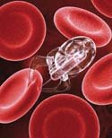
Call for Scientific Data on Applications of Nanotechnology and Nanomaterials used in Food and Feed

The European Commission has requested an initial scientific opinion from EFSA relating to the risks arising from nanoscience and nanotechnologies on food and feed safety and the environment. The request also asks to identify the nature of the possible hazards associated with actual and foreseen applications in the food and feed area and to provide general guidance on data needed for the risk assessment of such technologies and applications.

European Commission adopts Code of Conduct for Responsible Nanosciences and Nanotechnologies Research

Europe is in the vanguard of the emerging field of nanosciences and nanotechnologies (N&N), a developing field of science with the potential for major positive impact economically, socially and environmentally. Nevertheless, knowledge gaps remain about the impact of these technologies on human health and the environment, as well as issues relating to ethics and the respect of fundamental rights. This is why the Commission is today recommending to the Member States to adopt a Code of Conduct to govern research in this field.

European Commission gives grant to investigate transatlantic oversight of nanotechnology

Researchers at the London School of Economics and Political Science (LSE), Chatham House, Environmental Law Institute (ELI) and the Project on Emerging Nanotechnologies (PEN), an initiative of Woodrow Wilson International Center for Scholars and The Pew Charitable Trusts, have been awarded a $587,000 European Commission grant to conduct an international research project on regulating nanotechnologies in the European Union and United States.

Events: Nanomechanics for NEMS: scientific & technological issues


26-27 June 2008, Minatec, Grenoble, France

A workshop of the Observatory for Micro & NanoTechnologies
This workshop is devoted to a worldwide state-of-the-art on NEMS and nanomechanics. During two days, the most recognised leading researchers will display the current state of research on fundamental topics and associated technological developments, challenges to overcome, main teams involved, applications & market to be aimed. Through four lively sessions, leaving enough time to questions and debate, chairmen and speakers will outline a complete and synthetic view of the subject. This workshop was elaborated with the help and participation of Prof. M. Roukes (Caltech).

For more information visit: www.omnt.fr


Events: Nanotech Northern Europe 2008

23-25 September 2008, Bella Centre, Copenhagen, Denmark

Nanotech Northern Europe 2008 has opened its call for contributions. To be considered, for an oral or poster presentation, please submit an abstract via the event website at www.nanotech.net. The deadline for submissions is 29th February 2008. Topics include:

  • Sustainable solutions for energy and environment
  • Nanotechnology-enabled ICT
  • Nanobiotechnology and nanomedicine
  • Nanotechnology and Food
  • Safety and Risk Management

For more information please visit www.nanotech.net

Nanotech Week: European News

Nano.org

TU Delft invests 10 million euro in bionanoscience

The TU Delft launches a new Bionanoscience Department, which will be part of the Kavli Institute for Nanoscience.

The new department will work together with the existing departments of Nanoscience and Biotechnology, and will count 15 top scientists in the coming years. A strategic collaboration with the European Molecular Biology Lab EMBL will also be developed.

Nano-Tera.CH gets a boost

The EPF Council has decided to allocate 40 million francs to the Nano-Tera.CH initiative (5 million in 2008, 8 million in 2009 and 13.5 million in 2010 and 2011).
The nano-tera program is centered on the application of micro/nano-technologies to embedded systems design, with the goal of improving human conditions through the monitoring of the human body and the environment. The total funding for this program, on the order of 60 MCHF, will support multidisciplinary projects to create complex systems for health, security and environment.
This decision is excellent news, not only for researchers in this domain, but also for industrial partners, and it will be an opportunity to showcase Swiss dynamism in this area. The program, coordinated by EPFL professor Giovanni de Micheli, will be officially launched January 28 in Bern.

The MONA Nanophotonics Technology Roadmap now available

During 2 years (2005-2007), the MONA ("Merging Optics and Nanotechnologies") consortium has been working through workshops, symposia and expert interviews at establishing a roadmap for photonics and nanotechnologies in Europe.

Nanosafe2 releases its first dissemination report

This first report is about conventional protective devices such as fibrous filter media, respirator cartridges, protective clothing and gloves and their efficiency against nanoaerosols.

Nano2Life - The European Landmark in Nanobiotechnology

Nano2Life (N2L), the first European Network of Excellence in nanobiotechnology, will showcase its achievements to EC representatives and the scientific community in Brussels on February 26, 2008.

EU nanotechnology R&D in the field of health and environmental impact of nanoparticles

Being the first of its kind, this compilation has information of 106 projects, 14 of them are from the FPs which give around 32 million € in grants. The others 92 projects are from the EU Members States which spend around 47 million € in grants. This makes a total of some 79 million €.

Dutch trade union wants nanodebate

(In Dutch)

Manager Michiel Hartveld of the Dutch trade union FNV demanded openness on the presence of nanotechnology on the workplace from the side of industrial companies.

Transnational call for collaborative proposals in nanoscience

NanoSci-E+ is a body created specifically for the implementation of a transnational call for collaborative proposals in nanoscience wherein research agencies from 13 countries of the European Research Area (ERA) participate.

Research Project on Graphene Nanoelectronic Devices kicks off in 2008

Will graphene really take the semiconductor industry towards the "Beyond CMOS" era? Some answers to this key question are sought through experiment and simulation in a European research project on Graphene-based Nanoelectronic Devices called "GRAND".

Nanowire arrays think big

Nanotechweb

Feb 15, 2008

By Belle Dumé

A new bottom-up assembly method to make large-area nanoelectromechanical (NEM) arrays - each containing over 2000 single-nanowire resonators has been developed by researchers in the US. The technique is a practical alternative to top-down fabrication and the arrays could be used as multi-analyte biosensor chips.

NEM resonators are good candidates for making chip-based sensor arrays because they can sense ultralight masses. However, it is difficult to integrate nanowires into large arrays using traditional top-down techniques, such as optical lithography.

The new bottom-up technique was devised by Theresa Mayer of Pennsylvania State University and colleagues, and involves assembling thousands of chemically functionalized nanowire resonators and integrating them on a silicon chip. The finished nanodevices can bind specific biomolecules and so serve as sensors.

Mayer and colleagues begin by applying an alternating voltage between pairs of metal guiding electrodes patterned on a silicon chip. This produces spatially confined electric fields that attract the nanowires placed on the chip to specific regions.

The nanowires then align and drop one-by-one into wells patterned onto a sacrificial dielectric layer coated on top of the electrodes. The wells are slightly larger than the nanowires and are placed a few microns apart. This determines nanowire density, which can be as large as 1 million devices per square centimetre.

Next, the researchers deposit metal contacts onto the chip until the contacts fill small gaps in the sacrificial dielectric layer at the ends of each well. This mechanically and electrically connects the nanowires in the wells to the chip surface. Eventually, this technique will be used to connect to underlying silicon circuits, says Mayer.

Finally, the sacrificial layer is dissolved and any misaligned nanowires, not securely fastened to the chip by metal contacts, are washed away. This leads to a higher yield of assembled single nanowire devices over large chip areas.

"We used this assembly method to fabricate arrays of cantilevered silicon and metal nanowire resonators," Mayer told nanotechweb.org. "However, it is versatile and can be used to fabricate other types of nanowire-based devices as well."

The technique may also allow integration of many different types of nanowires functionalized to detect different target biomolecules made in large batches on fully processed silicon logic chips, added Mayer.

The team is now trying to extend its assembly technique to allow selective positioning of various types of nanowires in different locations on the chip. This will allow multiple biomolecule targets to be detected on the same chip. "We are also investigating new approaches to make an all-electrical interface to the silicon chip," said Mayer.

The work was reported in Nature Nanotechnology.

About the author

Belle Dumé is contributing editor at nanotechweb.org

Wednesday, 13 February 2008

Nanotechnology $1 trillion market by 2015

Nanotechnology Development Blog

20 December 2007

Bangalore Nano 2007 was recently held at Bangalore and it provided the opportunity to discuss the various aspects of the nanotechnology. According to Sir Keith O. Nions, Director General Science & Innovation, Dept. for Innovation, University of Skills in UK, the nanotechnology will have a global market of $1 trillion by the year 2015.

Industries such as automotive, steel, textile, energy, health, food, IT, paints, defence etc will provide enormous opportunities for commercialization of nanomaterials. Worldwide governments are now establishing new centres for commercializing new technologies.

In UK, government is funding more than 100 million pounds per annum for research on nanotechnology and government has open up 23 new centres for commercialization of the new technology produced by more than 1300 nanotechnology companies. UK has recently set up ISO technical committee of Nanotechnology.

Nanotechnology for producing clean technologies

Nanotechnology Development Blog

12 February 2008

A number of technologies are being used for producing and manufacturing number of items across the globe. Billions of amount being spent on using latest technologies for making them more environmental friendly. Lots of efforts are being taken for making zero pollution industries.

Nanotechnology has so far achieved many solutions but it is still unable to produce a few pollution free products. The scientists at the U.S. Department of Energy’s Argonne National Laboratory has recently come up with a new clean technology.

Scientists has come up with a scientifically elegant way to produce ethylene. Ceramist Balu Balachandran and his research team has devised a high temperature membrane through which ethylene can be produced directly from ethane. This new membrane removes hydrogen from ethane and the technology is absolutely pollution free.